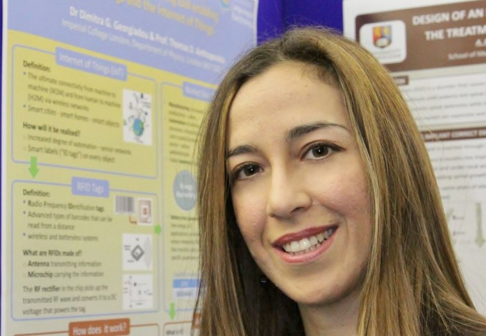
Dr Dimitra Georgiadou

An insider's account of the SET for Britain competition 2016, where early career researchers have the opportunity to present their work at Westminster
Monday, 7th March 2016, around 14:15, I arrive at Portcullis House Main Entrance, Westminster. The long queue of young people carrying poster tubes assures me I am in the right place. Among the co-tube-holders that wait to pass the security controls there is a diffuse feeling of excitement, anticipation, pride, honour. At the door of the Attlee Suite Mrs Sue Wharton, widow of Dr Eric Wharton, the founder of the SET for Britain competition, kindly welcomes us to the event. I locate my poster board number, hang it up, a very quick pass by the buffet for a little refreshment and the first visitor is already there. One of the judges, member of the Royal Society of Engineering, asks me to present my poster in 3 minutes as I would do to a High School pupil.
I start by introducing terms such as the Internet of Things (IoT), the ultimate connectivity of all electronic devices and appliances to an Internet “cloud”, and giving some examples of how its realisation will facilitate and secure the day-to-day living through: (a) live monitoring of health conditions, (b) fully automated “smart homes” that interact with their inhabitants like living organisms (for instance by dimming the lights according to mood and informing of the groceries that are running low or are about to expire in the fridge), (c) “smart tags and labels” that protect customers from counterfeited luxury or sensitive (e.g. pharmaceutical) products, to name but a few.
Then I refer to the quintessential element that lies in the heart of the IoT, namely the radio frequency identification (RFID) tag. This can be thought of as being an “advanced form of barcode” that can be read from a distance ranging from 1 cm to 10 m, depending on the operating frequency. Scientifically speaking, it is a microelectronic component comprising a chip and an antenna that is uniquely associated with each object and carries and/or transmits data wirelessly. Thus, the antenna can pick up an RF signal emitted from a base-station and not only harvest this energy to power the chip but also transmit the information stored in the tagged object. To do this one needs a so-called rectifying diode.
The judge wants to know more about my specific contribution to this very interesting application field. I am excited to explain the work I have undertaken during the last year within Professor Thomas Anthopoulos’ Advance Materials and Devices group in the Physics Department and Centre for Plastic Electronics of Imperial College London with funding I received from EPSRC’s Centre for Innovative Manufacturing in Large Area Electronics. I have been working on a novel, innovative technique, named adhesion lithography (a-Lith). This technique is expected to lower the fabrication cost of RF rectifying diodes used in RFID tags, accelerate their market uptake and open up the way to new applications, as thousands of tags could easily be produced by simple printing techniques on large area plastic flexible substrates without compromising their performance characteristics.
a-Lith, in principle, allows deposition of two dissimilar metals one next to the other separated by an extremely short channel, namely a 10-15 nm nanogap. This gap is formed after modifying the surface adhesion forces of one metal (e.g. aluminium) with an organic molecule and peeling off the weakest bound parts of the second metal (e.g. gold), simply by using a common Scotch tape. My first task was to automate this peeling step by setting up a “peeling machine” to prove that this technique has high potential to be scaled up from lab to industrial environment.
Apart from the nanogap fabrication step, I studied and optimised also the performance of RF rectifying diodes. To do this, I selected the most suitable materials, the types of the metals and a high mobility semiconductor, for instance Zinc Oxide or a Buckminsterfullerene, which has to be placed inside the nanogap. Then, current will flow only under forward bias direction with the device acting as diode that converts alternating current (AC) voltage to direct current (DC) voltage. This voltage can be used to power modern-day electronics. The comparative advantage of our nanogap diodes is that, in this geometry, charges can cross the active device channel faster and respond effectively to a much higher frequency alternating electric field than conventional “sandwich” structures. I inform the judge that I was recently awarded with a Marie Sk?odowska Curie fellowship to carry on research on this attractive topic.
Suddenly I hear a buzz all around. The photographers all run in the same direction. An MP has just entered the room and walks towards a poster. We keep ourselves very busy talking to different people during the next couple of hours. Looking back now I realise I did not use the same “storyboard” twice. Depending on the person I talked to, I adjusted the content and the level of my presentation: a brief and concise scientific explanation to the competition judges, a non-specialist summary-like discussion with the MPs and a more relaxed and friendly conversation with my peers.
Our session comes to an end with the announcement of the prizes for the three best posters by the sponsors of the event. The three winners get on stage to receive their prizes but we all feel we have won something this evening: a glimpse into the world of politicians and their encouragement to continue performing cutting edge research. Definitely, a day to remember!
Article text (excluding photos or graphics) available under an Attribution-NonCommercial-ShareAlike Creative Commons license.
Photos and graphics subject to third party copyright used with permission or © Imperial College London.
Reporter
Dimitra Georgiadou
Department of Physics
Contact details
Email: press.office@imperial.ac.uk
Show all stories by this author